
Summary on
CMOS Image Sensors for High Speed Applications
(Munir El-Desouki , M. Jamal
Deen , Qiyin Fang , Louis Liu
, Frances Tse and David
Armstrong )
Sensors 2009, 9(1),
430-444,Published: 13 January 2009
Introduction
For an Image to be captured 2 basic steps are involved
For an Image to be captured 2 basic steps are involved
- Image Acquisition
- Image processing
Recent advances in deep submicron CMOS technologies and
improved pixel designs have enabled CMOS-based imagers to surpass charge-coupled devices (CCD) imaging
technology for mainstream applications. The parallel outputs that CMOS imagers can
offer, in addition to complete camera-on-a-chip solutions due to being
fabricated in standard CMOS technologies, result in compelling advantages in
speed and system throughput. Since there is a practical limit on the minimum
pixel size (4~5 μm) due to limitations
in the optics, CMOS technology scaling can allow for an increased number of transistors
to be integrated into the pixel to improve both detection and signal
processing. Such smart pixels truly show the potential of CMOS technology
for imaging applications allowing CMOS imagers to achieve the image quality and
global shuttering performance necessary to meet the demands of ultrahigh-speed
applications.
In this paper, a review of CMOS-based high-speed imager
design is presented and the various implementations that target ultrahigh-speed
imaging are described. One of the main advantages of CMOS image sensors is
that they are fabricated in standard CMOS technologies, which allows for full integration
of the image sensor along with the processing and control circuits on the same
chip and at a low cost. This camera-on-chip system leads to reduction in power consumption, cost and sensor size and allows for integration of new sensor functionalities. Since
digital transistors take more advantage of CMOS scaling properties, digital pixel
sensors (DPS) have become very attractive. Such smart pixels truly show the
potential of CMOS technology for imaging applications allowing CMOS imagers to achieve
the image quality and global shuttering performance necessary to meet the
demands of ultrahigh-speed applications.
- Array Level Technique

(Array-Level Techniques)
Pixel-Level Techniques
Pixel-Level Techniques
A DPS(Digital pixel sensor) integrates an ADC into each pixel resulting in
a massively
Parallel readout and conversion that can allow very
high speed operation, where digital data is read out of each pixel.

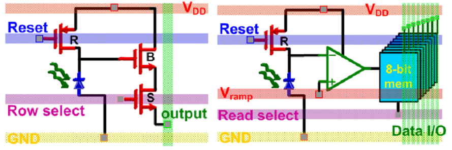
(3 MOSFET transistor) (Operational Amplifier) (DigitalOutput)
(Photo Diode)
Using a DPS(right side diagram) will only require one ADC conversion
cycle for all pixels in parallel, which results in a great increase in
capturing rate. The high speed readout makes CMOS image sensors suitable for very
high-resolution imagers (multi-megapixels) especially for video applications.
Analog
Readout Architectures
In order to achieve the fastest FR possible for a certain
high-speed experiment, a number of extremely fast consecutive images can be
captured and stored in analog form. By doing so, the inter-frame delay caused
by the ADC conversion time and array readout can be avoided. The FR (Frame
rate)only depends on the speed of the devices and transistors used within the
pixel, assuming a large enough illumination exists on the object being imaged.
Depending on the type of experiment and the Speed of capture, there will be a
minimum number of frames that is acceptable.
Ø Ultrahigh-Speed CMOS Imager can capture 8 frames at an
acquisition rate of 1.25 billion fps.
Ø Contain 38 transistor(complex circuit, Not included
here)
Ø The basic idea is to utilize 8 analog memory units to
temporarily hold 8 frames at a very high speed, avoiding the delay time in
analog-to-digital conversion and readout.( Things are done parallel, hence
delay time get reduced as compared to using 1 memory unit).
Conclusions
Existing results with
different CMOS imaging architectures have achieved thousands up to even
millions of fps(frame per second).By combining a number of different methods,
which include parallel per-column or
per-pixel ADCs, image compression, parallel output port readout, high readout clock rates and simultaneous capture and
processing, researchers have managed to push frame-rates to 10,000 fps.
Using an ultrahigh-speed imager design for a 1-D line-scan
imager can increase the number of consecutive images that can be captured at
rates of over a billion fps.
Research on high speed image capturing using Cmos and other
technology is going on largely and the time to acquire and process the high speed
image is getting decreased over the years
Reference: www.mdpi.com/journal/sensors.
Reference: www.mdpi.com/journal/sensors.
No comments:
Post a Comment